|
|

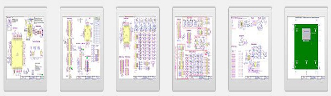


Board Design
The typical board that Project Development works on requires
sorting through issues such as:
- Multiple power supplies and voltage levels.
- High speed signals that must be placed and routed correctly.
- Analog and digital sections that must be placed and routed correctly.
- Components and traces that generate heat which must be dissipated.
- Differential and single ended signals that must maintain the correct impedance.
- Mixed signal boards with connector positions or allowable component placement areas that don't make any sense.
- For most boards space is at a premium, finding a spare millimeter or a few thousands of an inch is the norm.
- Budgets that demand a variety of design compromises.
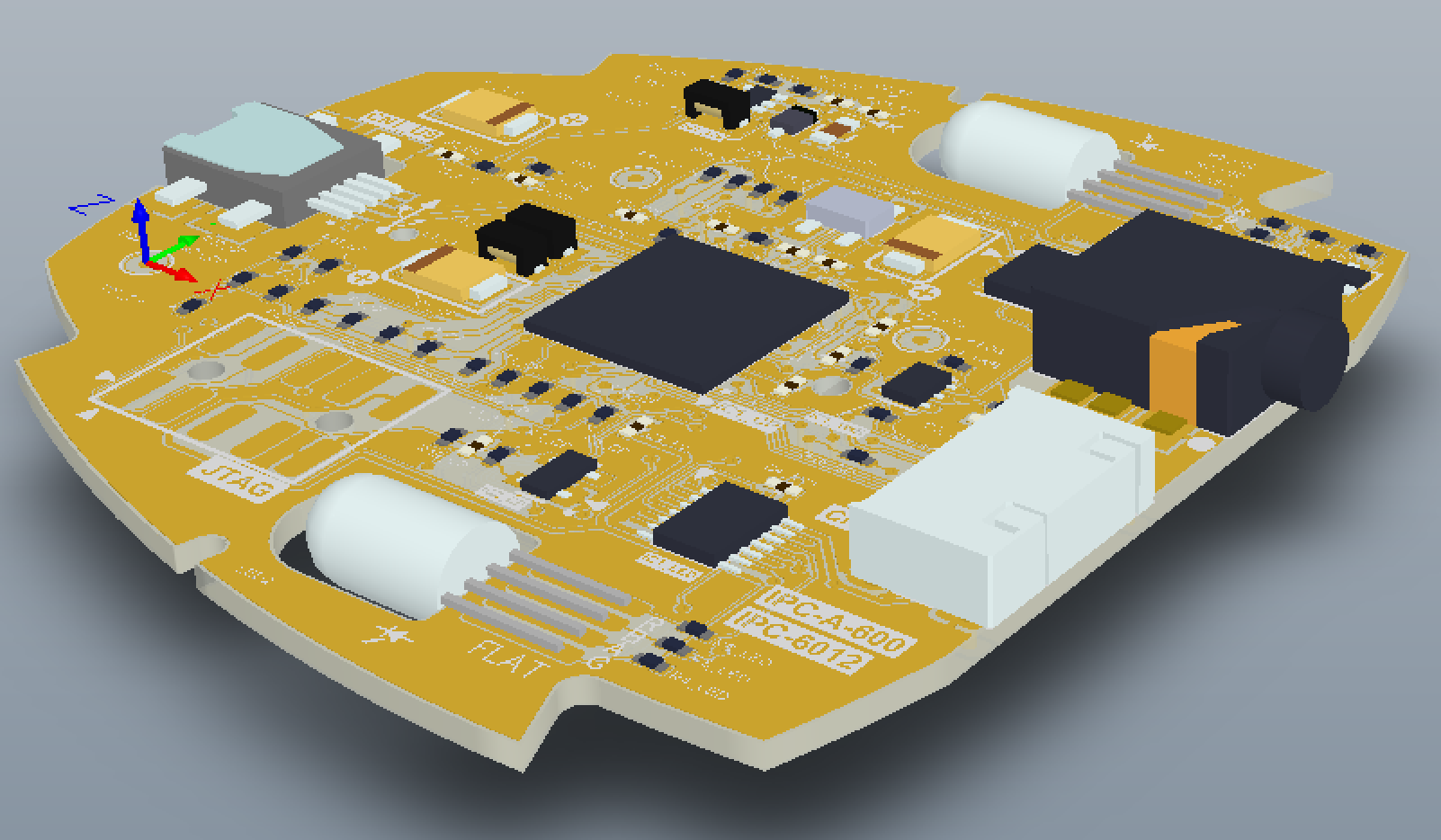
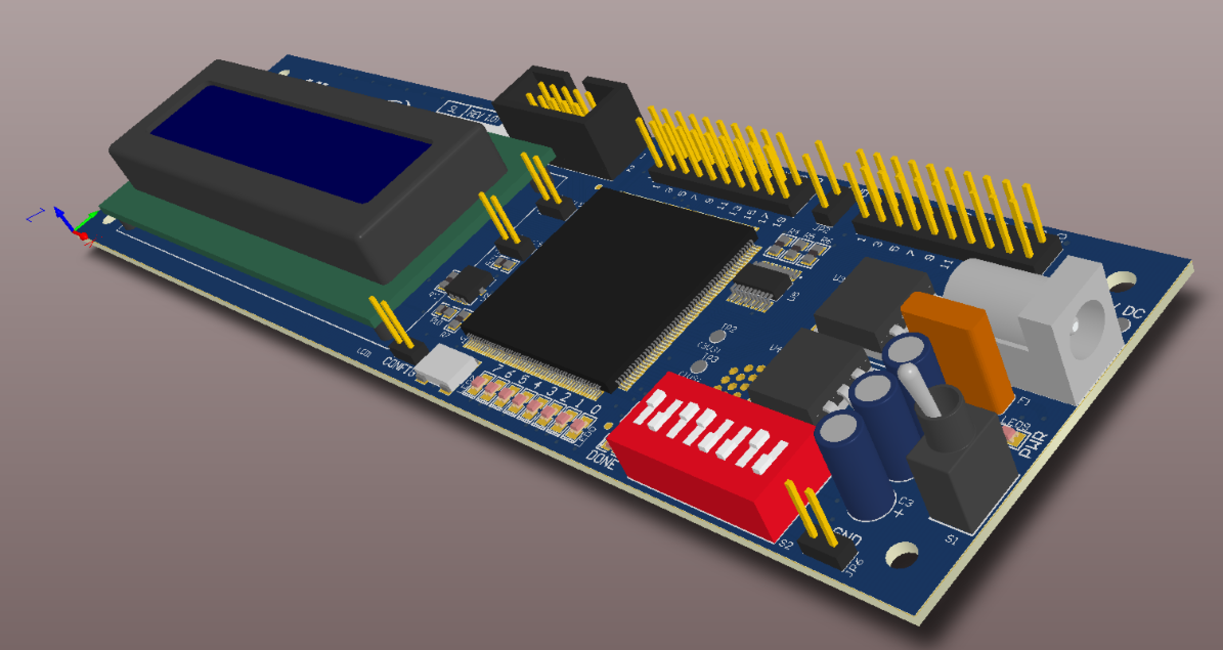
Electronic 3D clearance checks with quickly
generated shapes or STEP files
Solutions
- Design for manufacturing and assembly without problems.
- Mechanical CAD and PCB CAD are integrated to examine enclosure fit and component clearances.
- Gerber File editing
- Conversion of Gerber manufacturing files to CAD files.
- Autorouting
- Schematics revised or drafted.
- Component Search
- Bill of Materials creation or administration.
- Board fabrication/assembly quote process administration.
- Teleconferencing allows board to be seen in real time.
© 2020 All Rights Reserved Project Development LLC